Wireless Power Transfer
Power Electronics Report · Palina Kuzmina and Berry Xu · May 2026
This report details the design, simulation, and physical implementation of a wireless power transfer (WPT) system utilizing resonant inductive coupling. A transmitter circuit converted DC power into a high-frequency AC waveform using an NPN solid-state switch, which drove a primary transmission coil. An inductively coupled secondary coil received the transmitted power, which was rectified and filtered to supply a DC load. The LTSpice simulation achieved an estimated efficiency of 48.91% at a coupling coefficient of K = 0.7. The physical prototype yielded approximately 2% efficiency, highlighting the impact of parasitic capacitance, skin-effect losses, and non-ideal coupling.
Introduction
Wireless power transfer has become increasingly prevalent in modern consumer electronics because it offers a convenient way to charge devices without cables. Instead of electrical connectors, a wireless charger transfers energy through an electromagnetic field via inductive coupling between two coils. The purpose of this project is to design and build a basic wireless charger that demonstrates electromagnetic induction and power transfer.
Theory
Wireless chargers operate on the principle of magnetic induction. According to Ampere's law, a magnetic field is generated around a current-carrying wire. When a wire is wound into a loop, peak magnetic flux is concentrated around the middle. Faraday's law states that a changing magnetic field through a coil induces a voltage proportional to the rate of change of magnetic flux.
A wireless charger consists of two wound coils. Alternating current passes through the primary coil, or transmitter. When the secondary coil—the receiver—is placed near the primary, the changing magnetic field induces a current in the receiver coil.
Transmitter
The transmitter circuit converts DC to a high-frequency AC waveform using a switching solid-state device.
The transmitter and receiver form a resonant circuit. The two coils form an effective inductor, and the transmitter has a capacitor placed in parallel. In this configuration, the voltage and current in the coils can become much larger, strengthening the magnetic field so the receiver picks up more energy. Resonance transfers more power with less wasted energy and permits more distance or misalignment than plain inductive coupling. This is called resonant inductive coupling.
Receiver
The secondary coil is connected to the receiver. The coil ratio N2/N1 determines whether the voltage is stepped up, stepped down, or kept the same. The input is then fed into a rectifier and filtering capacitor to produce DC voltage.
Design and Implementation
Parts
Only the wireless charging receiver coil, wireless transmission coil, and 30 V, 3 A SOT32 NPN transistors were bought. The rest of the materials were sourced from JLab.
| Part | Price | Amount |
|---|---|---|
| Wireless charging receiver coil | $13.06 | 1 |
| Wireless transmission coil | $6.19 | 1 |
| 30 V, 3 A SOT32 NPN transistor | $8.16 | 2 |
| 1 µF capacitor | N/A | 1 |
| 1N5817 diode | N/A | 4 |
| 8.2 Ω power resistor | N/A | 1 |
| 1 kΩ resistor | N/A | 2 |
| 0.001 µF capacitor | N/A | 2 |
| 10 µH inductor | N/A | 2 |
Solid-State Switch Rationale
The transmitter uses a 30 V, 3 A SOT32 NPN bipolar junction transistor (BJT) as the primary solid-state switch. The choice between a BJT and MOSFET is driven by frequency, power capability, and drive simplicity. While MOSFETs generally offer faster switching and lower conduction losses at high frequencies, an NPN BJT was selected for its sufficient current-handling capability and simplified current-controlled base drive for a fundamental oscillator topology.
Circuit Simulation
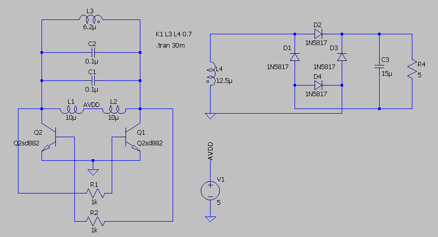
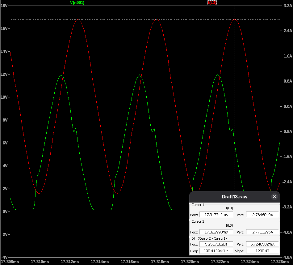
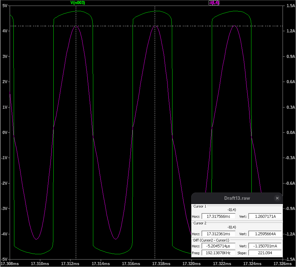
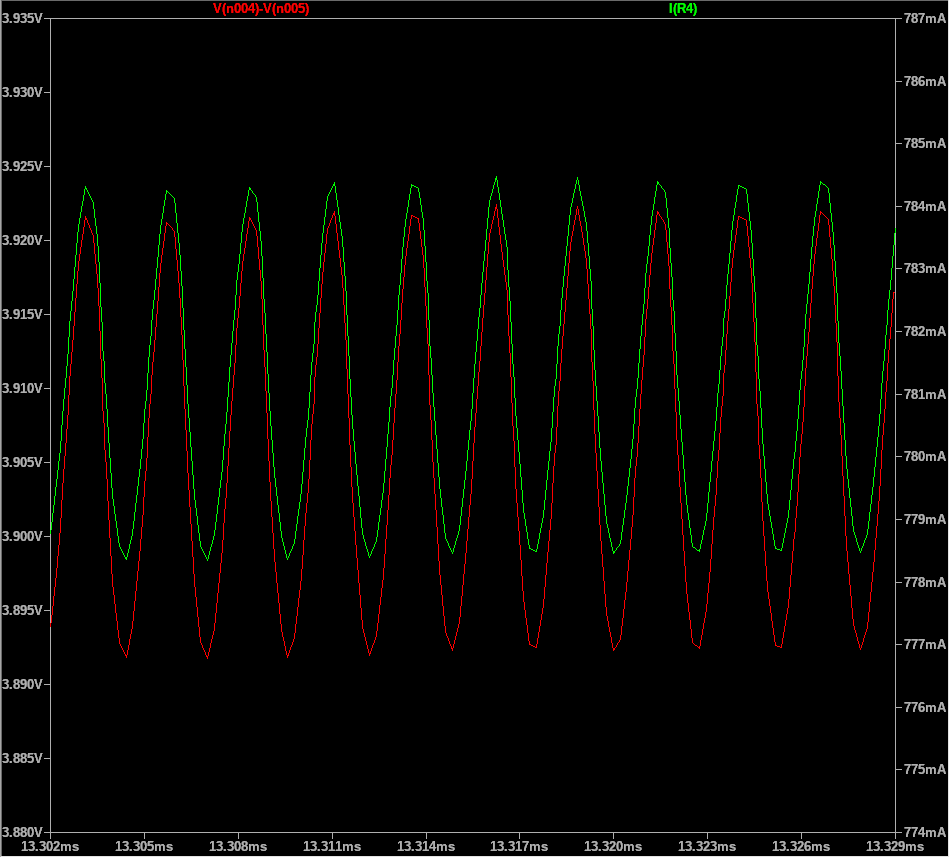
Circuit Implementation
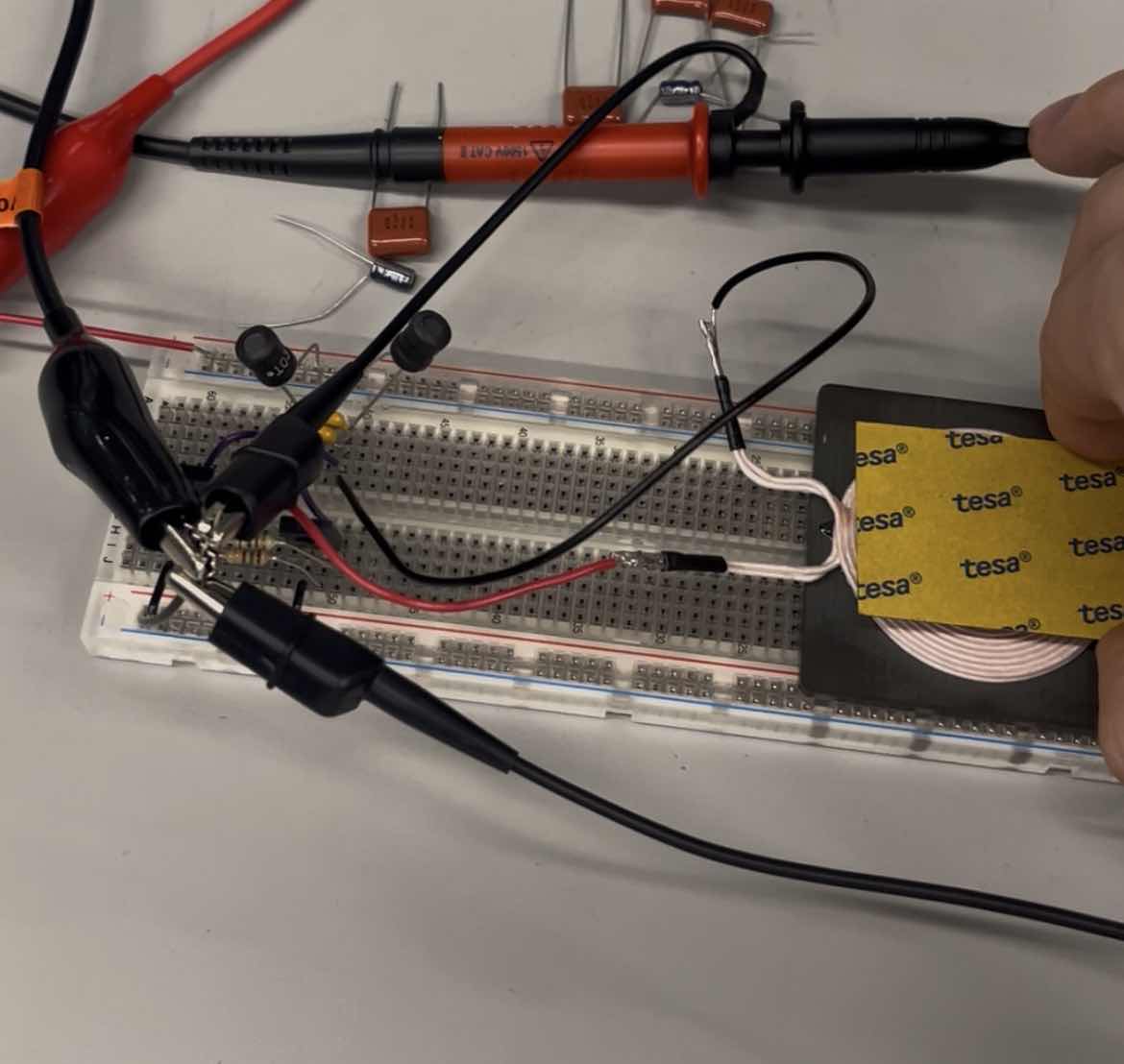
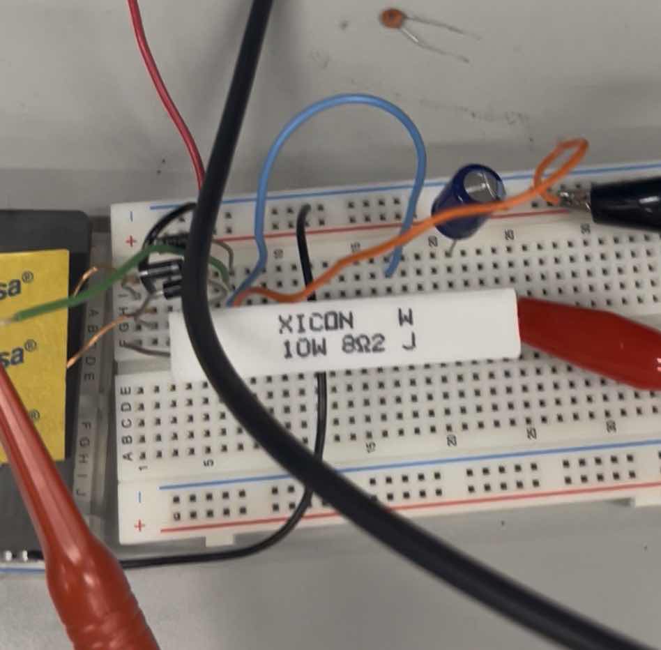
Results and Discussion
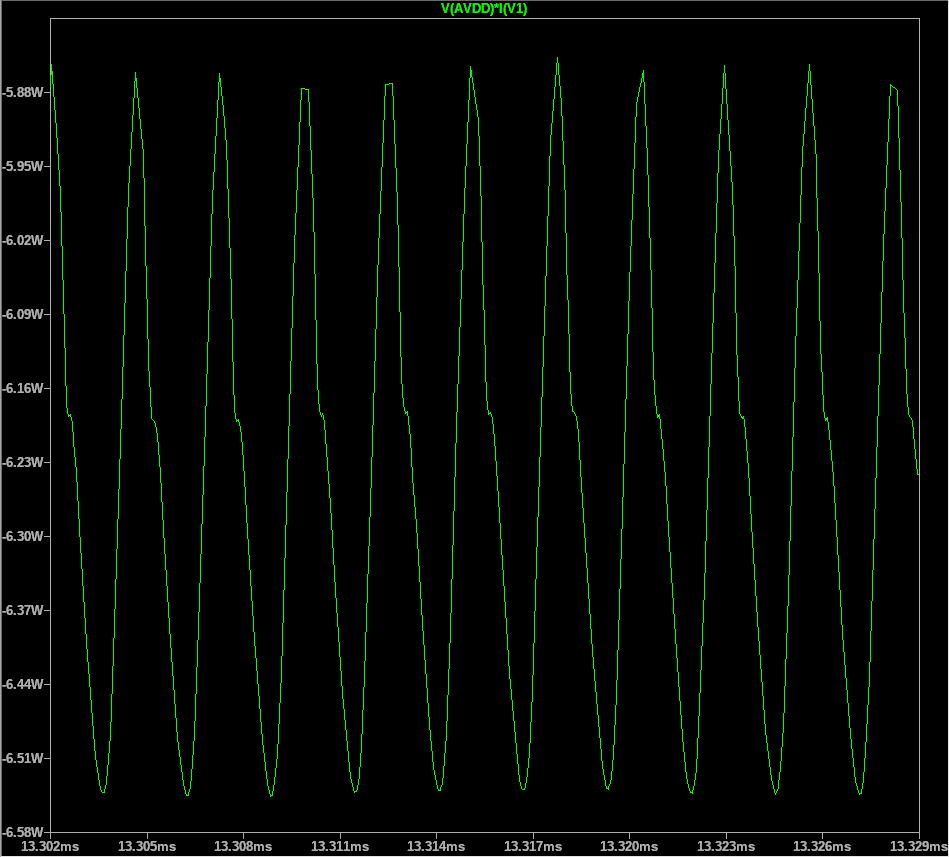
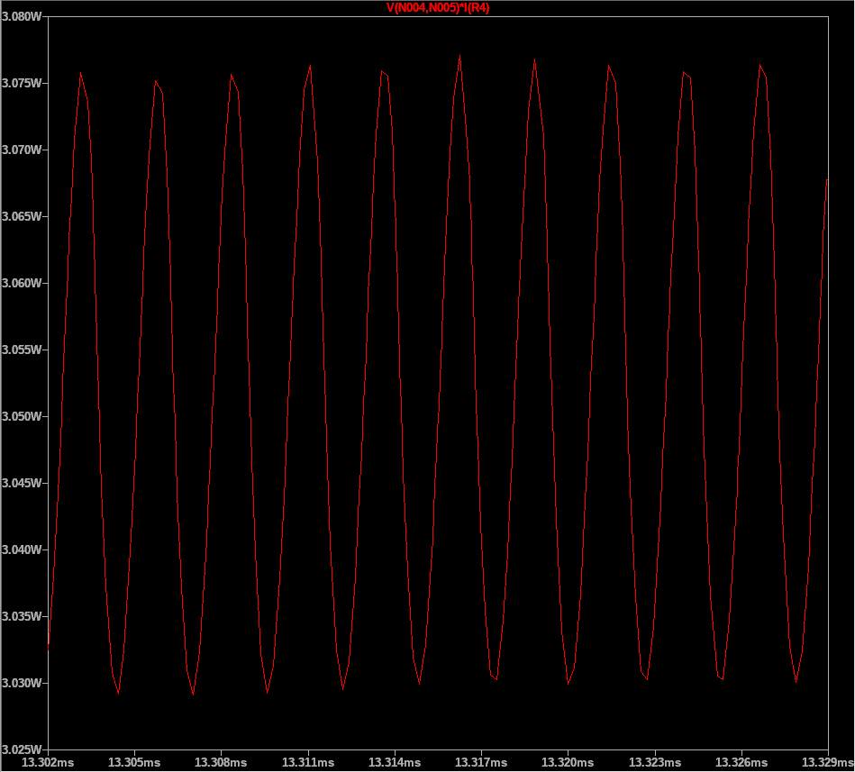
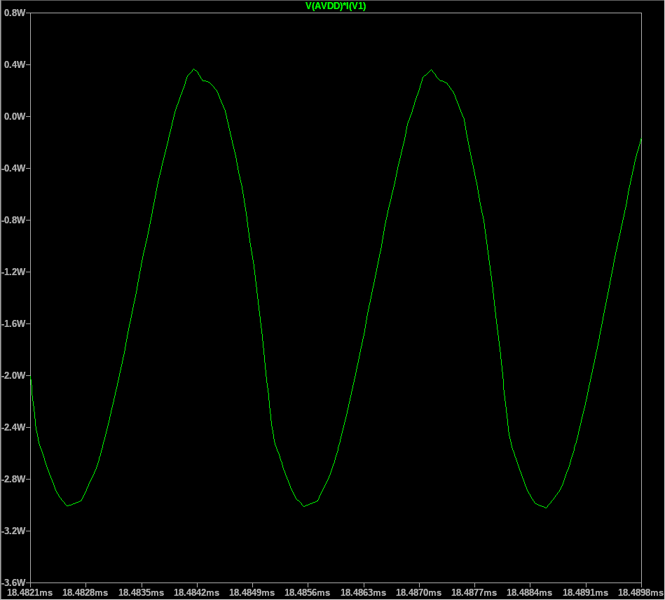
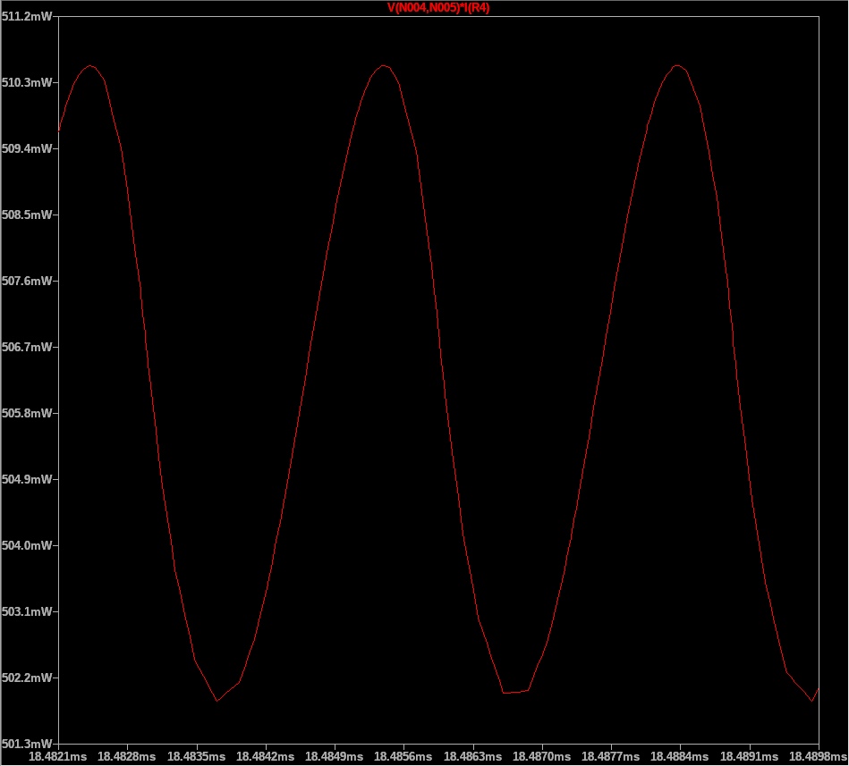
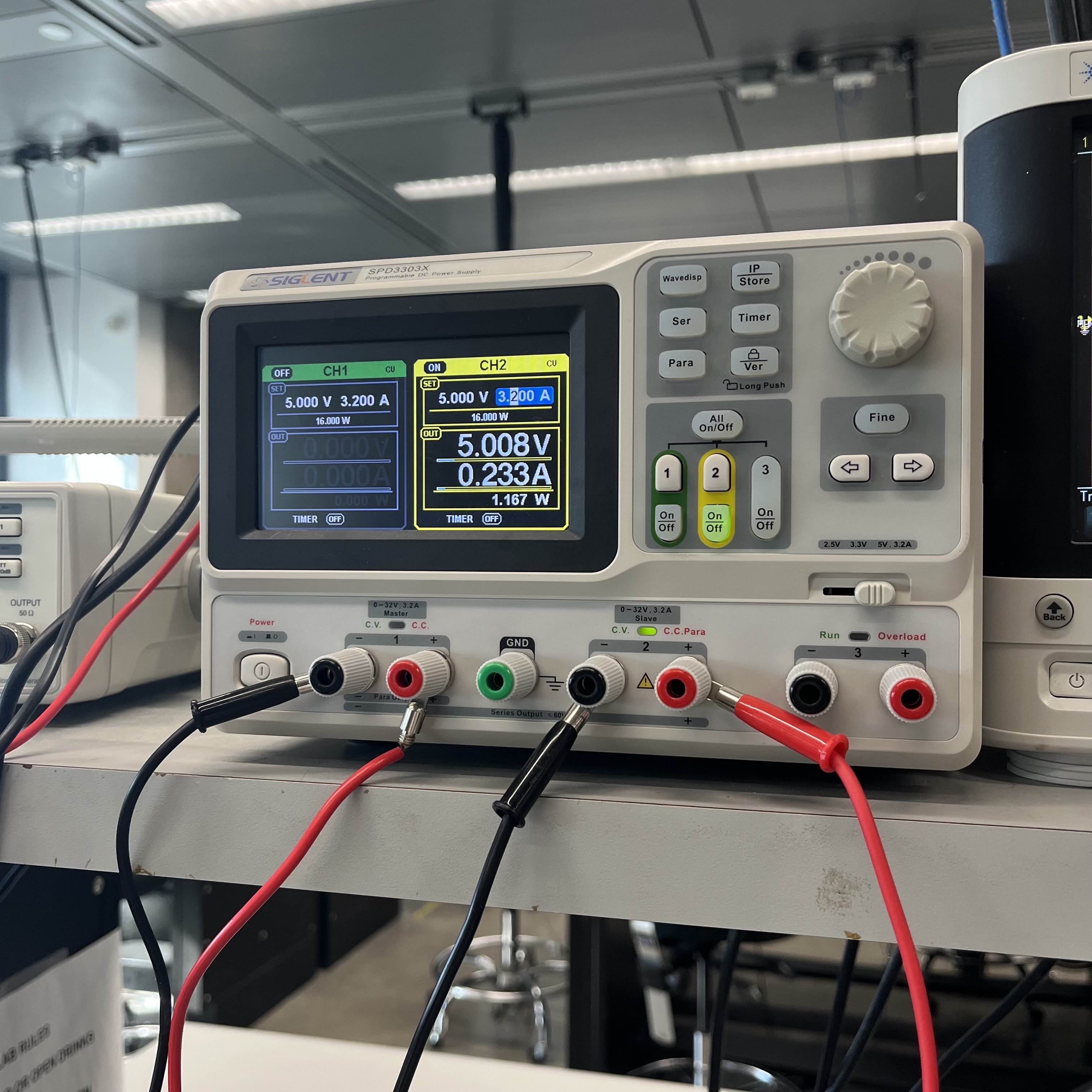
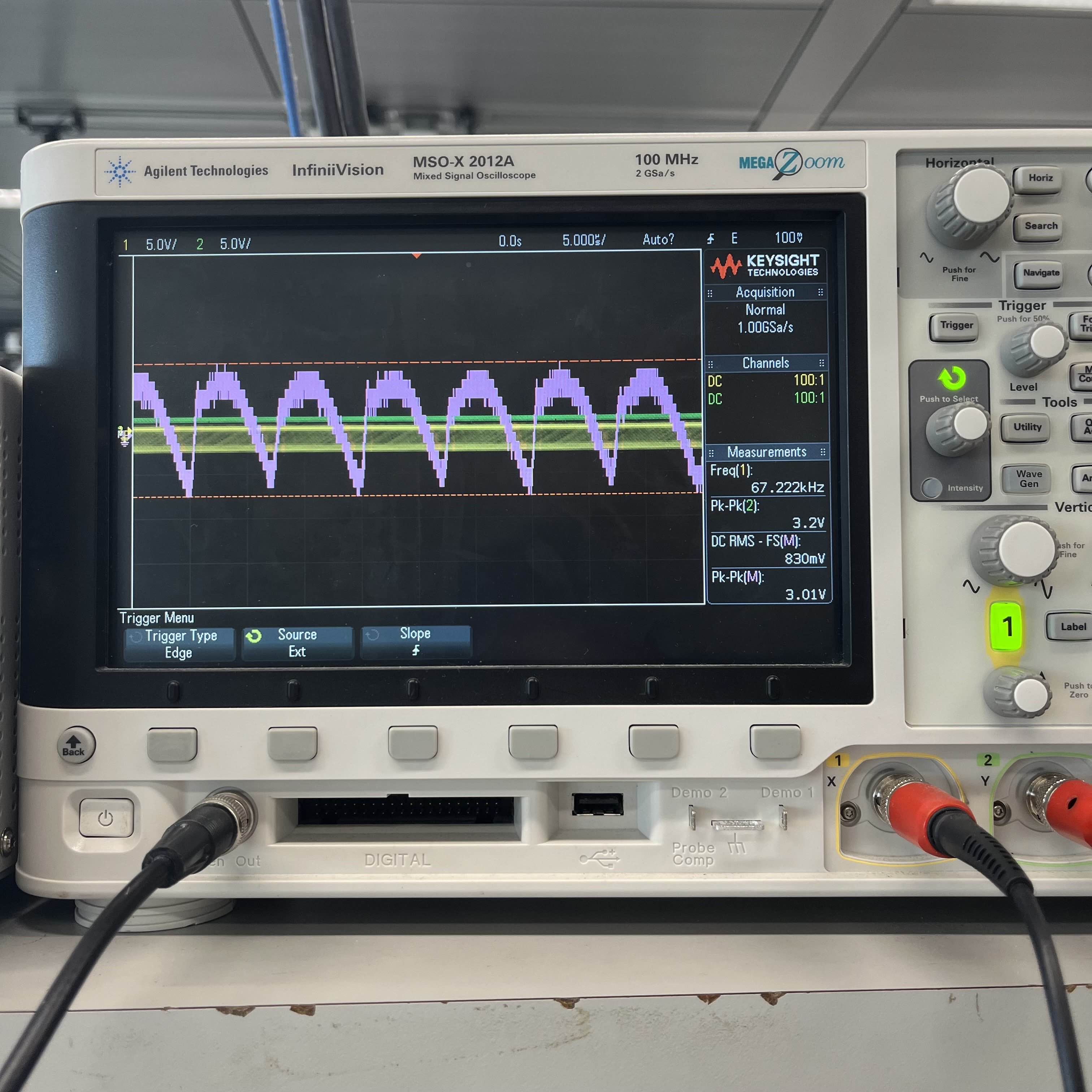
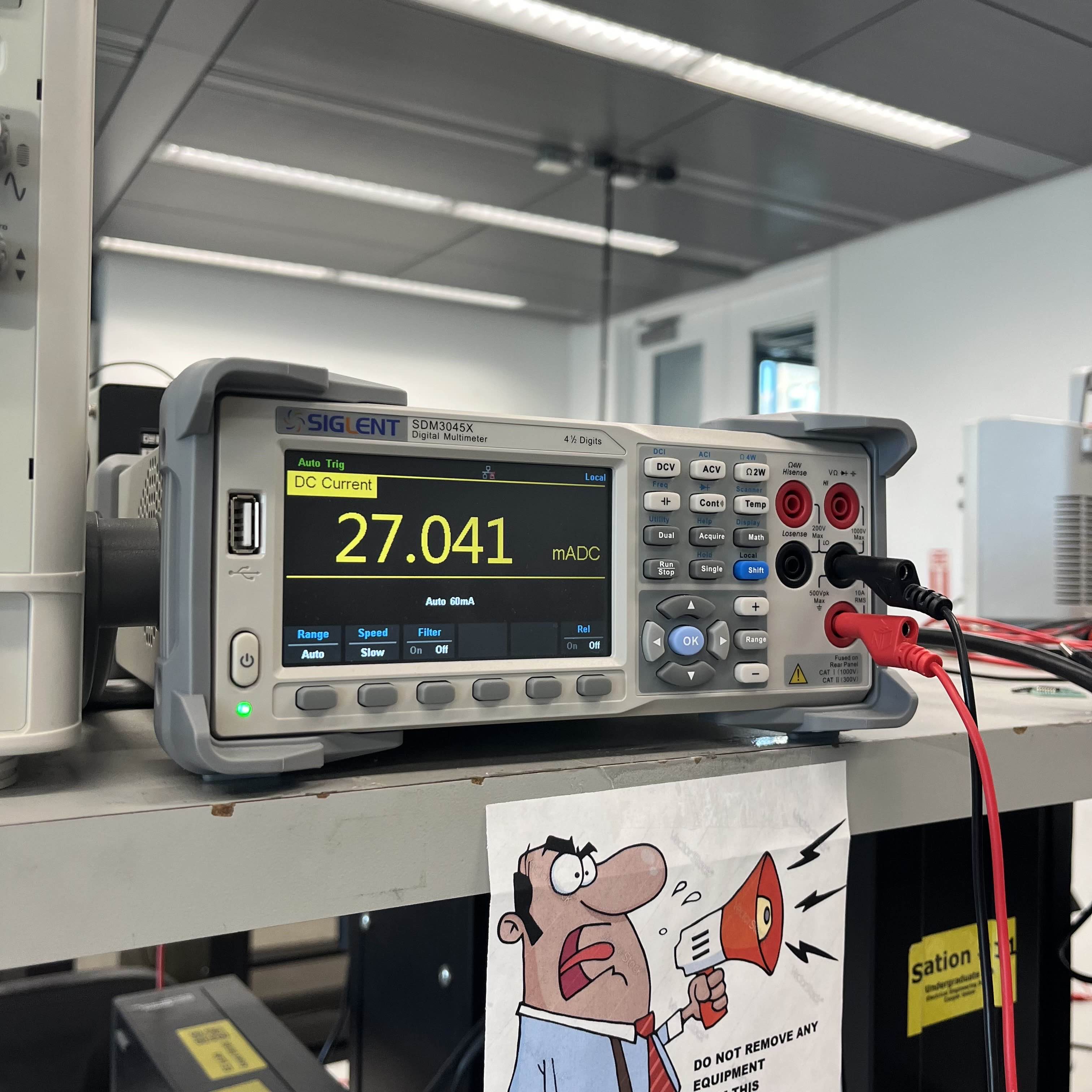
In simulation, at K = 0.7, Pin = 6.2367 W and Pout = 3.0507 W, with an efficiency of 48.91%. At K = 0.3, Pin = 1.3201 W and Pout = 505.98 mW, with an efficiency of 38.3%. In the physical circuit, Pin = 1.16686 W and Pout = 0.02241 W, with an efficiency of approximately 2%. The measured output was Vpp = 3.01 V and Vrms = 830 mV.
Conclusion
The prototype's low efficiency resulted from several effects that were not represented adequately in the idealized simulation: breadboard parasitic capacitance disrupted resonance, the thin and undersized receiver coil produced high DC and AC resistance, imperfect coil alignment and sizing reduced magnetic coupling, and the rectifier's diode drops consumed a large portion of the small received voltage. A future version should use a tuned PCB instead of a breadboard, a larger receiver coil wound with lower-resistance wire, better-matched and carefully aligned coils, and a lower-loss rectification method. Feedback could also adjust the transmitter frequency to maintain resonance as the load or coil position changes.